Developing an electronic device involves so many fronts that it is understandable to focus heavily on circuit design, stack-up, trace routing, impedance control, component selection, thermal dissipation, and the assembly process. However, there is one decision that often appears near the end of the specification phase: the surface finish for the exposed copper.
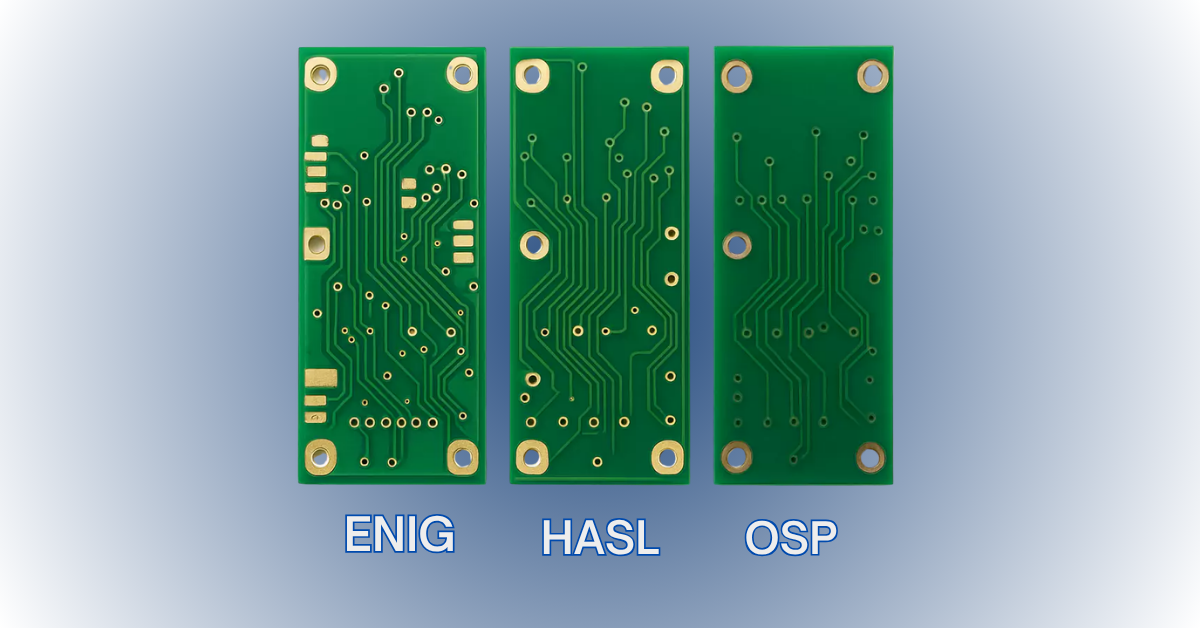
The most common options—ENIG, HASL, and OSP—are readily available, leading many to view them as simply different price tiers. But that is not the case. It is worth remembering how critical this decision can be, as the surface finish directly influences solderability, flatness, shelf life, joint reliability, and, in specific applications, even the electrical performance of the board.
Types of Surface Finishes for Printed Circuit Boards
HASL – Hot Air Solder Leveling
The copper surface is coated with molten solder and subsequently leveled using hot air knives.
It is a robust, widely used, and relatively low-cost solution with excellent solderability. Its primary limitation is surface coplanarities and unevenness, which can become a major issue for fine-pitch components, BGAs, QFNs, and high-density layouts.
ENIG – Electroless Nickel / Immersion Gold
Consists of an electroless nickel layer covered by a thin layer of immersion gold.
Its outstanding flatness, solderability, and oxidation resistance make it particularly attractive for BGAs, QFNs, fine-pitch footprints, and applications requiring long shelf life.
However, ENIG is not a universal fix. The quality of the deposition process is critical; an inadequate process can lead to defects like Black Pad (where the nickel layer beneath the gold corrodes and turns dark, compromising solder joint integrity).
OSP – Organic Solderability Preservative
Instead of a metallic coating, OSP applies an ultrathin organic film to shield the copper from oxidation.
It offers superior surface flatness and serves as an attractive alternative for specific SMT workflows and high-volume runs. Its main drawback is that protection relies heavily on strict storage conditions, handling care, and thermal exposure during multi-pass reflow operations.
Other Surface Finishes:
-
Immersion Silver (ImAg)
-
Immersion Tin (ImSn)
-
ENEPIG (Electroless Nickel / Electroless Palladium / Immersion Gold)
-
Electrolytic Gold / Hard Gold
These specialized finishes cater to niche applications. As IPC (the global trade association establishing standards for electronic design, manufacturing, and assembly) highlights, there is no single universal surface finish: every option presents specific trade-offs that must align with the target application.
Problems Associated with Poor Surface Finish Selection
Selecting the wrong surface finish or utilizing a substandard plating process can trigger a cascade of issues:
-
Manufacturing: Poor coplanarity, solder paste printing defects, insufficient wetting, bridging, or cold solder joints.
-
Reliability: Joint degradation, corrosion, or mechanical failures following thermal cycling.
-
Electrical Performance: A degraded joint or contact interface can introduce parasitic electrical resistance, localized heating, intermittent connections, or loss of signal integrity.
-
Aggressive Environments: Exposure to moisture, atmospheric pollutants, and sulfur compounds can accelerate corrosion. IPC has extensively documented phenomena like creep corrosion linked to specific finishes and ambient conditions.
-
Operational Lifespan: Latent defects that pass early functional testing may manifest as catastrophic field failures months or years into operation.
Implications for Electrical Performance
This is where surface finish selection becomes critical. While it may not drastically alter the overall power consumption of a board, there are specific domains where the finish forms an integral part of the electrical model.
In physical contact interfaces, surface degradation increases and destabilizes contact resistance. Under high current loads, this resistance translates into power dissipation and localized thermal hot spots.
For high-speed digital and RF designs, another phenomenon emerges: the physical properties of the conductive surface layer directly affect signal attenuation.
As signal frequencies increase, the skin effect forces electrical current to concentrate predominantly near the outer surface of the conductor rather than through its center. Consequently, the chemical composition, roughness, and structure of the surface layers transition from a pure manufacturing concern into a core factor of signal integrity analysis.
Studies published by IPC demonstrate measurable differences in insertion loss across different surface finishes in high-frequency structures. When a design is sensitive to signal loss, the surface finish must be included in electromagnetic simulations and loss budget calculations.
Criteria for Selecting the Right Surface Finish
Selection should never be driven by unit price alone or by chasing the “highest quality” option on paper. The goal is to identify the finish that yields optimal performance for the specific application, assembly process, and expected operating lifespan.
Consider these factors before finalizing your specification:
-
Geometry and Density: BGA/QFN pitches, fine-pitch requirements, and surface coplanarity tolerances.
-
Assembly Process: Number of reflow passes, selective soldering, wave soldering, and rework requirements.
-
Storage and Logistics: Shelf life duration, humidity controls, handling protocols, and warehouse conditions.
-
Reliability Demands: Thermal cycling range, target operating lifespan, and harsh environment exposure.
-
Electrical Functionality: Whether the pad serves solely as a solder joint or doubles as a sliding/mating electrical contact.
-
High-Frequency Demands: Operating frequency, signal loss budgets, controlled impedance parameters, and trace geometry.
-
Total Lifecycle Cost: Evaluating potential costs associated with scrap rates, rework, field defects, warranty claims, and overall lifecycle expenses.
In Conclusion
A small line item in your fabrication print warrants a significant engineering decision. Surface finish selection must be integrated into your Design for Manufacturability (DFM) reviews, as well as signal integrity and reliability evaluations, from the earliest stages of hardware design.
ENIG, HASL, and OSP are not merely three pricing options on a PCB quote—they are engineering parameters that dictate how your hardware is built, how it performs, and how long it survives in the field.
*Article based on real-world engineering cases.